Element Six and Orbray Scale Up Wafer-Scale Single Crystal Diamond Production
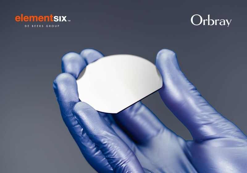
Advanced materials leaders Element Six (E6) and Orbray Co., Ltd. have entered the next commercialization phase of their strategic partnership, shifting focus from initial R&D to the volume manufacturing of Wafer-Scale Single Crystal diamond (WSCTM). The collaboration has successfully yielded a highly repeatable fabrication process for 3-inch synthetic single crystal substrates, providing an order-of-magnitude increase in total area and surface uniformity over conventional mosaic or small-scale diamond plates. The partners have also confirmed that development of larger 4-inch diamond substrates is officially underway to meet industrial semiconductor line demands.
To target immediate commercial integration pathways, the companies are finalizing production lines for smaller wafer form factors optimized for specific electronic and thermodynamic workloads. Substrates measuring 2 inches are nearing finalization for advanced epitaxial growth applications, while a parallel run of 2-inch wafers engineered for high-power thermal bonding is transitioning to high-volume manufacturing. This volume production will be anchored at Element Six’s world-class Chemical Vapour Deposition (CVD) synthesis facility located in Gresham, Oregon, leveraging Orbray’s proprietary precision jewel cutting, grinding, and sapphire/diamond growth technologies to ensure sub-nanometer surface roughness.
The scale-up aims to alleviate the chronic sub-component supply bottlenecks currently delaying the hardware rollouts of next-generation critical infrastructure. Synthetic single crystal diamond’s ultra-high thermal conductivity, wide bandgap, and high carrier mobility make it a highly sought-after substrate for extreme-power computing environments. By establishing a reliable domestic 2-inch and 3-inch industrial supply chain, the E6-Orbray partnership expects to accelerate the market adoption of diamond electronics across 6G wireless infrastructure, high-power radio frequency (RF) military components, deep-space sensing arrays, advanced thermal management backplanes, and spin-defect-based quantum hardware platforms.
The official commercial press release from Element Six outlining the manufacturing milestone can be reviewed here. For an alternative operational overview detailing jewel-processing optics and precision grinding metrics, review Orbray's technical updates here.
June 16, 2026
Related Intelligence

Test of USydney article with HTML.
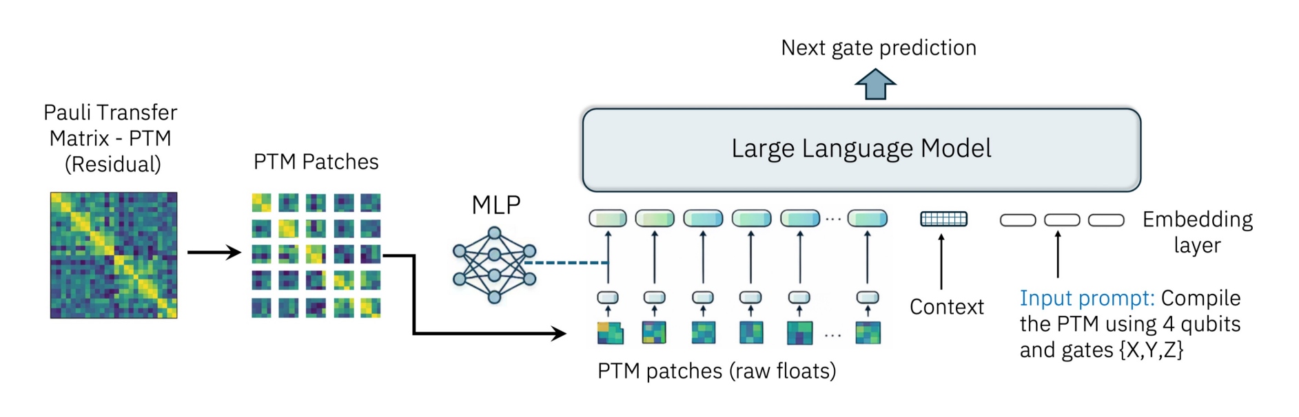
MIT and IBM Project Quantum Unity Operators into Language Model Latent Spaces for Multimodal Circuit Synthesis
July 11, 2026

ETH Zurich Combines Superconducting Qubits with Mechanical Resonators to Build Vibrating Quantum RAM
July 11, 2026

Google and Fraunhofer Launch Global Calls for Early Fault-Tolerant Algorithms and Enterprise Use Cases
July 11, 2026

Who’s News: Strategic Appointments at Photonic, Aliro Quantum, Florida Atlantic University, QuSecure, Quantum Elements, and QAI Ventures
July 11, 2026
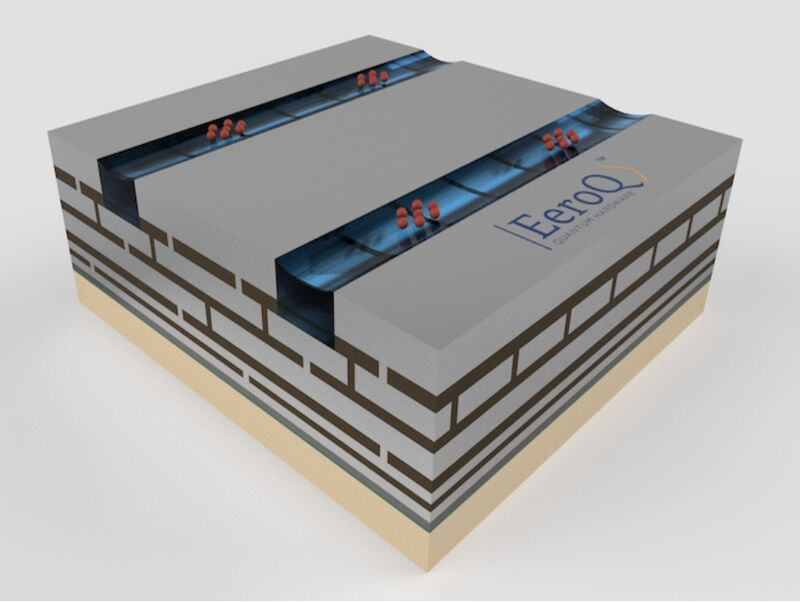
EeroQ Validates CMOS-Controlled Electron Shuttling on Superfluid Helium for All-to-All Qubit Routing
July 11, 2026