PsiQuantum Unveils 8×8 Optical Circuit Switch Demonstration Vehicle Derived from Silicon Photonics Quantum Architecture
PsiQuantum has developed an 8x8 optical circuit switch (OCS) using their silicon photonics platform, originally for quantum computing, but now repurposed…
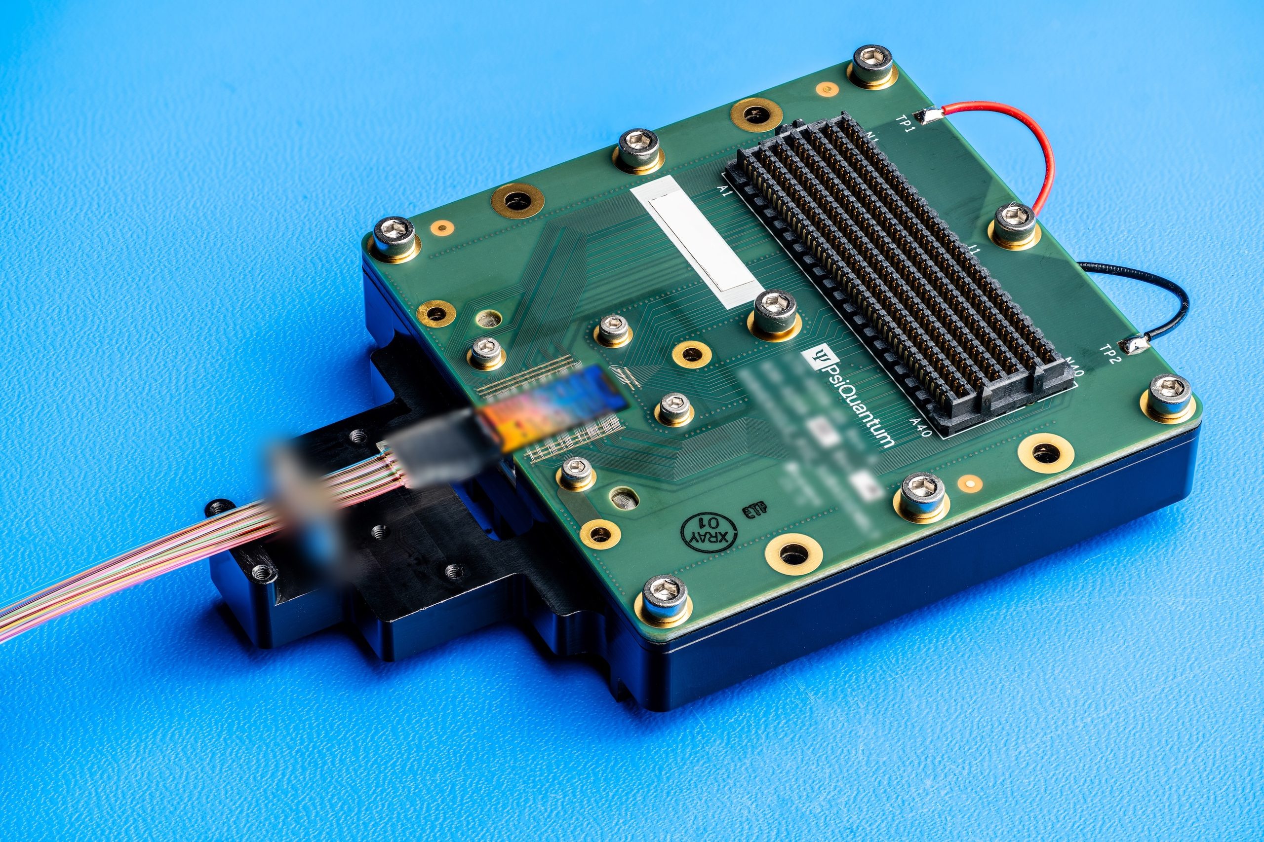
PsiQuantum has introduced an 8×8 radix optical circuit switch (OCS) built on the low-loss silicon photonics manufacturing platform the company originally developed for utility-scale fault-tolerant quantum computing. While engineered primarily to direct optical qubits within quantum processors, the demonstration vehicle is targeted at interconnect bottlenecks in high-density classical artificial intelligence (AI) cluster fabrics. By sampling hardware to prospective enterprise customers, PsiQuantum is establishing commercialization pathways for its fabrication processes ahead of utility-scale quantum deployments, leveraging domestic manufacturing initiatives formalized under an agreement with the U.S. Department of Commerce.
Switching Mechanics and Waveguide Platform Architecture
The OCS demonstration unit repurposes the passive optical waveguiding layer engineered to prevent single-photon loss inside PsiQuantum's quantum computing architecture. Rather than relying on power-intensive optical amplifiers to maintain transmission, the switch routes classical light beams through low-loss silicon waveguide channels using standard foundry manufacturing flows. For its core quantum processors, PsiQuantum uses a distinct high-speed routing design incorporating thin-film barium titanate (BTO) at the 300 mm wafer scale. The classical AI switch intentionally omits this BTO layer, prioritizing straightforward monolithic integration on standard silicon to facilitate immediate customer sampling while preserving the advanced material system for cryogenic quantum systems.
Demonstrated Silicon Photonics Performance Targets | ||
Operational Metric | Measured Value | Network System Impact |
Radix Density | 8×8 Port Matrix | Establishes direct fiber-to-fiber cross-connect pathways. |
Insertion Loss | 1.2 dB (Minimum 1.0 dB) | Avoids the thermal burden and noise of optical amplifiers. |
Inter-Channel Crosstalk | 40 dB Isolation | Suppresses phase noise and optical spillover between channels. |
Switching Latency | < 3 ms | Enables dynamic runtime circuit topology reconfiguration. |
Dual-Use Commercialization Realities and Fault-Tolerant Roadmaps
Commercializing classical networking hardware represents a deliberate dual-use strategy to monetize photonic manufacturing assets while long-term quantum platforms remain in development. Sampling the 8×8 switch provides prospective data-center operators an early evaluation vehicle, with formal commercial product lines scheduled for disclosure in the coming months. However, capturing volume market share in high-performance computing clusters requires scaling beyond an 8×8 matrix toward higher port counts without degrading total loss budgets during automated fiber packaging. Furthermore, while near-term optical interconnect revenue supports company operations, PsiQuantum's primary technical milestones remain tied to solving single-photon generation, high-fidelity optical entangling gates, and cryogenic fault-tolerant quantum error correction.
Details regarding the switching architecture and commercial sampling are outlined in the official PsiQuantum OCS Announcement here.
October 28, 2026
Related Intelligence

Test of USydney article with HTML.
EPFL Demonstrates Millimeter-Wave-to-Optical Transducer with 67% Internal Efficiency
November 10, 2026
Why Quantum Hardware Needs Its Own Threat Model
November 9, 2026
Physics Reports Analysis Evaluates Emergence of Hybrid Semiconductor–Superconducting Qubit Architectures
November 9, 2026
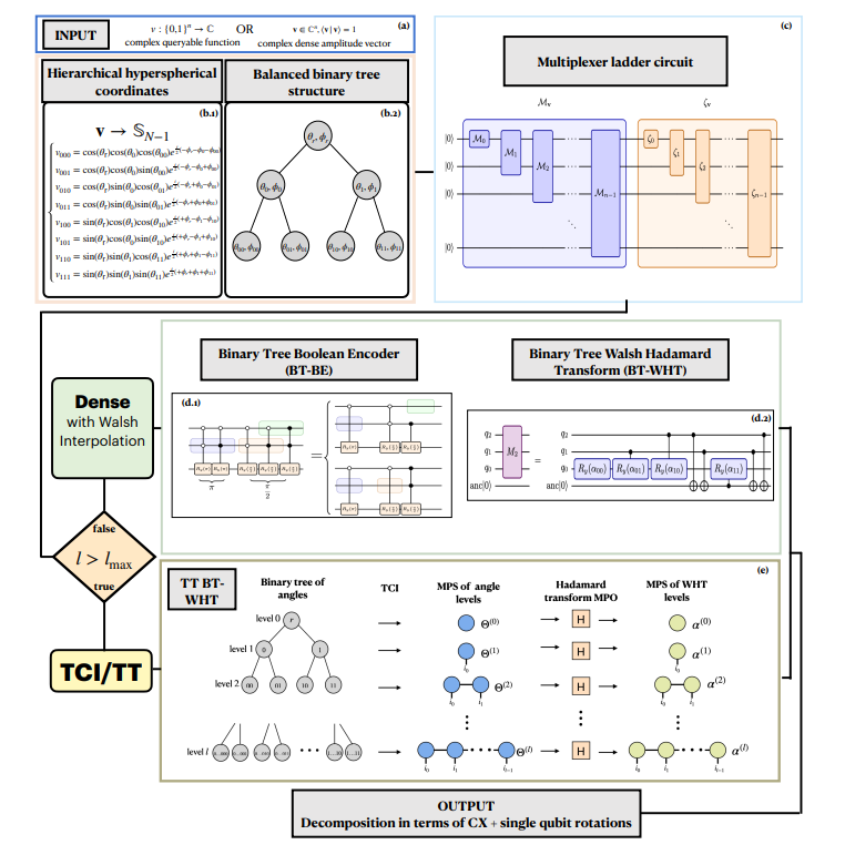
DLR Develops Scalable Unitary Data Encoding Beating Exponential State-Preparation Depth
November 9, 2026
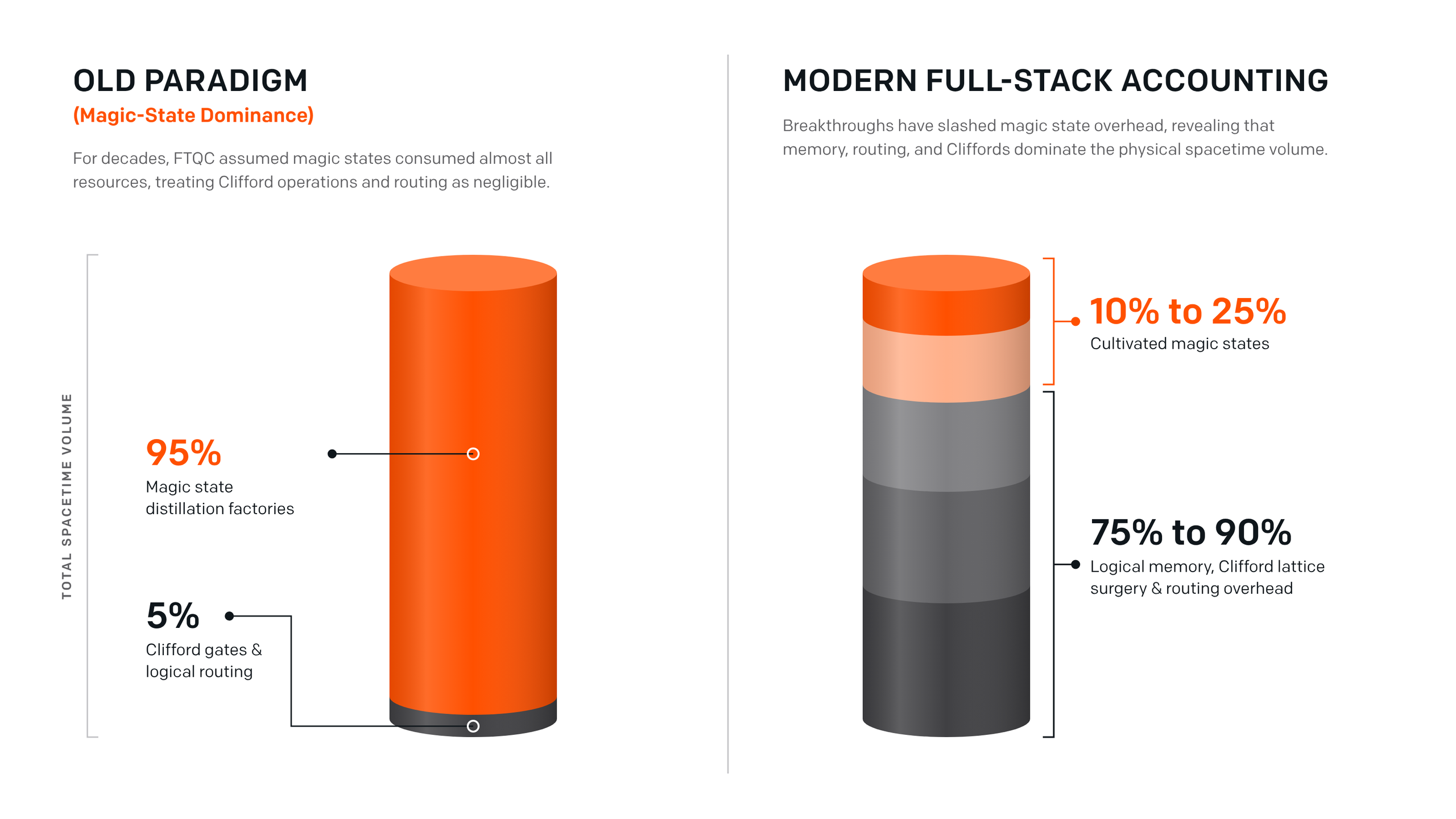
IonQ and Classiq Outline Architectural Trade-Offs in Fault-Tolerant Resource Estimation
November 9, 2026